|
|
Hardware
The following are the hardware components that make up the LED Clock. Because of the large size of the LED displays, each pair of displays is mounted on its own PCB. There is a separate PCB for the hours, minutes, and seconds digits. The PCBs are identical for each section. Jumpers on the PCBs are used to select the desired display function. In addition, only one of the PCBs (the seconds digit) contains the GPS engine used for timing.
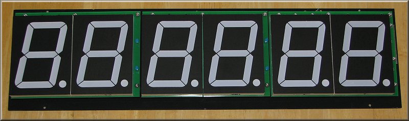
Shown below, is the front of the display. Discrete LED's are used to form the colon used between each display. Each board operates of 18VDC. The relatively high voltage is required because each segment of the display is made up of 5 chip LED's in a series. The forward drop voltage of the 5 blue LED chips is nearly 16.5 VDC. NOTE: The bubbled plastic on the front of the LED displays is a protective cover that is removed when installed in the enclosure.
|
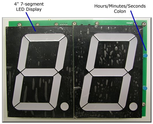
Front of Display
|
Shown below, is the rear of the seconds display with its GPS receiver. Note the addition of a large heat sink and 5 VDC regulator. In the original design, a linear regulator on the PCB provided the 3.3VDC to the embedded controller and GPS engine. However, because the GPS engine and active antenna require 115mA and the display operates from 18VDC, the regulator needed to dissipate 1.7 watts. The PCB heat sink trace wasn't large enough to dissipate the heat and the regulator operated at nearly +80°C. Although it is designed for +85°C, it didn't allow for much design margin. A good old LM7805 acts as a pre-regulator for the 3.3VDC regulator. In the next revision of the PCB, I'll use a switching regulator.
|
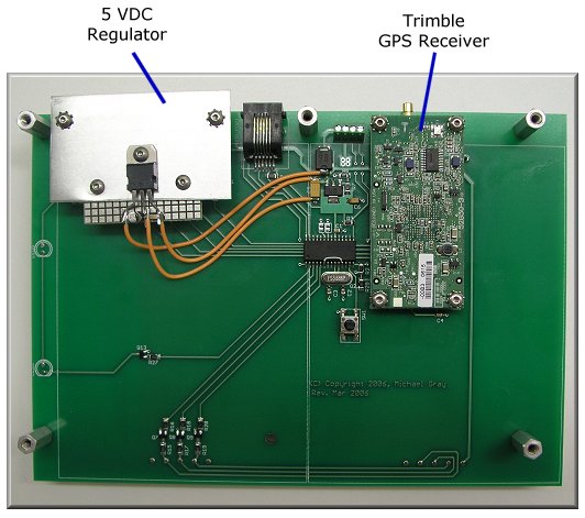
Master Clock Display
|
Shown below, is the rear of the PCBs for the minutes and hours display. Note the LM7805 pre-regulator isn't required because only the PIC embedded controller is powered on these boards. Since the PIC only requires a few milliamps of current, the 3.3VDC regulator doesn't get warm, even from the 18VDC main supply.
|
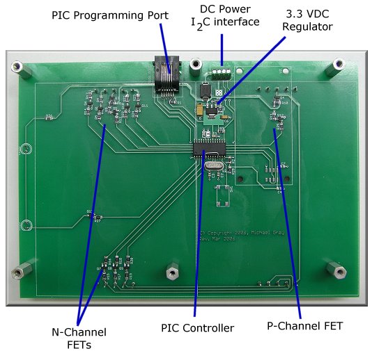
Slave Clock Display
|
Each of the PCBs is mounted to a large base plate. The base plate is press board painted in ultra flat black.
|
Clock Modules on Base Plate
|
Rear of the base plate showing the power and communication wiring. The modules utilize an I2C interface to communicate.
|
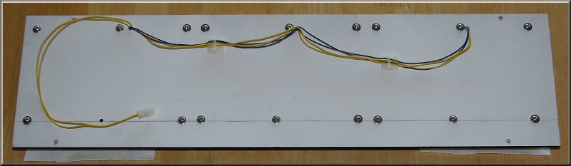
Rear of Base Plate |
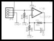
Schematic / PCB Layout
For best quality, print the schematic on a single 8½ x 11" sheet of
paper in landscape mode using your favorite graphics application.
NOTE: There were white wire and component value changes that are not
reflected in the schematics and board layout provided below. The
change will be incorporated into the design information as time permits.
 |
 |
|
Schematic
(Graphic - GIF) |
PCB
Layout
Top Layer
(Adobe PDF) |
PCB
Layout
Bottom Layer
(Adobe PDF) |
Additional information on viewing the PCB artwork, PCB tools, and
component libraries is available in the Technology section. |