


|
|
|
|
|
|
|
Design 2 This power converter is a general design that can be used in other projects. It is an all surface mount circuit that boosts or steps up a lower voltage to a higher voltage, in this instance 12.0 VDC. The device is capable of providing 300mA in a 1½" x 1½" package from a nominal 5 volt supply. The switching regulator operates near 92% efficiency. With the additional on board filtering, the output ripple is less than 10mV at the 1.4MHz switching frequency. The use of an output filter is preferred over the use of an LDO (Low Drop Out) regulator after the output of a switching regulator. The switching frequency is typically many octaves higher than then GBW (Gain Band-Width) product of the error amplifier in a linear regulator. Because of this, the linear regulator provides little to no ripple rejection. The modern linear regulator generally provides 50 - 60 dB of ripple rejection at 120 Hz (the typical frequency of a full wave rectifier). 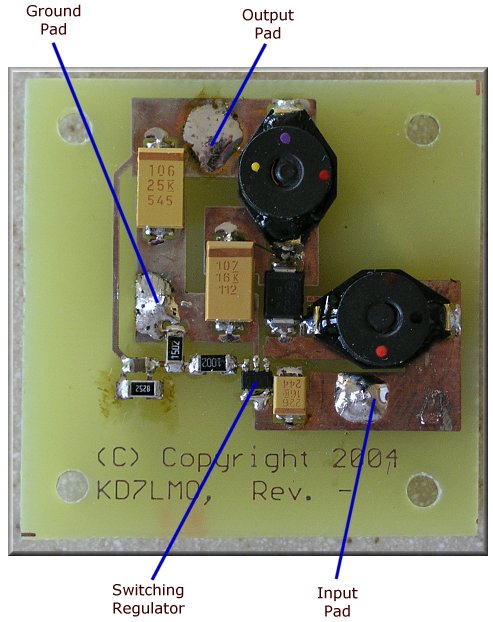 Low Ripple DC/DC Boost Regulator. Theory of Operation The LT1613 is a current mode, internally compensated, fixed frequency step-up switching regulator. DC power in the range 0.9 to 10.0 VDC is provided at the input pad. Inductor L2 is switched on and off at a 1.4MHz rate. During the on switch period, current flows through the inductor to ground. During the off switch period, the collapsing magnetic field of the coil generates a voltage higher than the input. This voltage is rectified by the high speed Schottky diode D1 and filtered by low ESR (Effective Series Resistance) capacitor C2. An additional filter comprised of L3 and C3 reduces the output ripple to less than 10mV. The output voltage is set by the voltage divider R2 and R3. C1 provides a phase lead and R1 additional FB (Feed Back) pin isolation to allow the use of lower cost, small ceramic capacitors or very low ESR tantalum capacitors. Although this design used tantalum capacitors, C1 and R1 were included to improve transient response from load changes. As with all switcher designs, circuit board layout and component selection is critical. The data sheet for the parts provide great detail on layout and component selection. Power Converter Schematic / PCB Layout For best quality, print the schematic on a single 8½ x 11" sheet of paper in landscape mode using your favorite graphics application.
|
|
Copyright © 2001-2009, KD7LMO |
|
Web space provided by ESS, Inc. for all your consulting needs. |

