|
|
Power Amp
Design Depreciated - This design has been replaced
with the next version of the HF-APRS hardware, however, this section is retained for historical reference.
Shown below is the HF amplifier mounted in an aluminum housing. The
housing was machined from a solid block of material and provides RF
shielding as well as a heat sink for the final stage of the PA. The
circuit is designed to operate from 8.5VDC. The amplifier operates in
a class A mode. Although less efficient than a class AB amplifier
design, the circuit is linear enough to operate without an output filter.
The input power level is adjusted so the second harmonic is -30dBc or less
than the carrier. With the second harmonic at -30dBc, the third
harmonic is typically -35 to -40dBc less than the carrier. All other
harmonics and non-spurious output levels are -60dBc or better. Future
designs may require an output filter as the FCC has recently changed the
spurious output requirement to -42dBc or better.

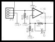
HF Power Amplifier
Theory of Operation
Nominally, the PA requires an input level of
-20dBm. Resistor R1 provides a 50 ohm
input match to the output of the exciter stage. The input signal is
amplified by two identical +14dB stages. The LM6624 is a 1.5 GHz GBW
(Gain Band Width) product op-amp. R4/R5 and R9/R10 set the gain of the
stage. A single amplifier stage is capable of +35dB of gain, but a
very conservative design divided the gain into two stages. L2/L3 and
C11-C14 provide input power de-coupling. Input bias is set by the
resistor divider R2/R3 and R7/R8. Capacitors C1, C3, and C5 provide
intra-stage AC coupling. Finally, series resistor R6 and R11 provide
matching between the stages.
The LMH6718 op-amp is used as a high current driver for the PA. L4 and
C9/C15 provide input power de-coupling. Input bias is set by the
resistor divider R12 and R13. Capacitors C5 and C7 provide intra-stage
AC coupling. The LMH6718 provides up to 200mA of drive current with a
130MHz of bandwidth and 6dB of gain.
The NTE342 is a silicon NPN epitaxial planer type transistor designed for RF
power amplifiers. It is designed for VHF band applications, but works
down into the HF bands with proper feedback. U3, the LP2981 linear
regulator provides +5VDC to bias the output transistor for class A
operation. The shutdown pin is used as a PTT (Push-To-Talk) control.
The DDS in the synthesizer is used to key the RF energy on and off to
prevent spurious output (key clicks). R14, R15, and R16 set the input
bias to the device. C19 and C20 bypass RF energy to ground to prevent
interference with the LDO. C8 and R17 provide feedback to greatly
reduce gain in the HF band and prevent oscillation of this VHF device.
L6 is an RF choke that feeds the collector of the PA. The 1:3 turn
ratio output transformer includes 7 turns on the primary and 21 turns in the
secondary.
The input and output ports are SMA type connectors to provide a good quality
RF connection and light weight suitable for a balloon flight.
Schematic / PCB Layout
For best quality, print the schematic on a single 8½ x 11" sheet of
paper in landscape mode using your favorite graphics application.
 |
 |
|
Schematic
(Graphic - GIF) |
PCB
Layout
Top Layer
(Adobe PDF) |
PCB
Layout
Bottom Layer
(Adobe PDF) |
Additional information on viewing the PCB artwork, PCB tools, and
component libraries is available in the
Technology section.
|