|
|
PCB
- Printed Circuit Board
A PCB, or Printed Circuit Board, offers a number of advantages over wire
wrapped or perf board assembly. The PCB allows the use of fine pitch,
surface mount components, a smaller footprint, more rugged assembly, ease
of duplication, and a
more professional final product. The
following is a step-by-step guide to creating a PCB using a positive,
photo resist process. An entire kit consisting of pre-sensitized PCBs,
chemicals, UV lamp, and etching tank is available from MG
Chemicals. The kit is also available through distributors such
as Mouser
and Digi-Key.
 Safety
It should go without saying, but I'll say it anyway, this stuff can be
dangerous. Making PCBs requires chemicals that are heated, UV light,
and sharp cutting tools. At a minimum, wear rubber gloves, safety glasses
or a face shield, and work in a well ventilated area. Safety
It should go without saying, but I'll say it anyway, this stuff can be
dangerous. Making PCBs requires chemicals that are heated, UV light,
and sharp cutting tools. At a minimum, wear rubber gloves, safety glasses
or a face shield, and work in a well ventilated area.
Create the
PCB layout The Eagle schematic capture, PC board layout, and auto router
application is utilized
to created the project PCBs. The software package is available from CadSoft.
CadSoft offers a freeware version of the tool for Windows and Linux as
well as professional versions at a very reasonable cost. After the
printed circuit board layout is generated, it is printed on a overhead
projector transparency. A box of transparency sheets for laser or
inkjet printers are available at most office supply stores. TIP - When printing
on the transparency,
select the highest resolution and darkest print option on your printer to
create dense trace lines.

Sample PCB artwork.
Additional information on viewing the PCB artwork, PCB tools, and
component libraries is available in the
Technology section.
Expose the
Board After the PCB artwork is printed on the transparency, it is laid
on the pre-sensitized PCB. A pre-sensitized PCB has a layer of
green or blue ink that is sensitive to UV light. Any portion of the
ink that is exposed to the light will come off the board when placed in a
chemical developer bath. The exposure time for the MG Chemicals boards are 5
minutes. The quality of the board is effected by the exposure time,
so a stop watch is handy when exposing the board. TIP - To hold
the transparency sheet on the surface of the board, place a piece of glass
on top of the board. This will ensure the trace lines are sharp.
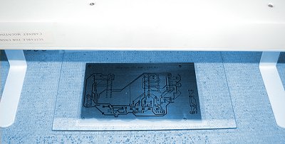
PCB
exposure under UV light.
Develop
PCB Pattern After the PCB has been exposed to UV light it is placed in a
weak solution of developer or Sodium Hydroxide. Using a foam brush,
gently brush the surface of the board. The development cycle will
typically require 1 to 2 minutes to remove the ink that was exposed to UV
light. The unexposed ink will remain on the PCB. After
development, carefully inspect the traces and wash the board with water. TIP
- Warm the developer solution to 75-80°F before developing the
board. This will greatly accelerate the development cycle and
prevent the removal of narrow width traces in the extended development
time of a cold solution.
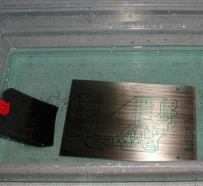
PCB
development bath.
|