

|
|
   |
|
|
|
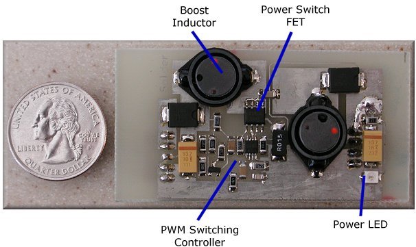
Design 1 This power converter is a general design that can be used in other projects. It is an all surface mount circuit that boosts or steps up a lower voltage to a higher voltage, in this instance 13.0 VDC. The device is capable of providing 3 amps in a 1½" x 2½" package. The switching regulator operates near 90% efficiency and the power FET doesn't require a heat sink with minimal input voltage and full output load at +85°C.  Switching Power Converter. Theory of Operation DC battery power in the range 2.95 to 16.0 volts is provided on the IN terminals. Diode D1 provide reverse polarity protection. The LM3488 switching controller operates in a SEPIC (Single Ended Primary Inductance Converter) mode. The MMDF3N03 power FET, 6.8uH L1 and L2 inductors, and D2 diode step-up or step-down the input voltage to the desired output. R8 and C1 provide filtered power to the LM3488 controller. R1 sets the switching frequency. R5, R6, R9, and the BSS138 FET provide a power down input. When Pin 3 of the IN terminal is pulled low, the regulator shuts down. Tantalum capacitors C5 and C7 provide filtering. R2 and R3 form a divider network to reference the output voltage to 1.24 volts. C2 provides high frequency coupling to reduce output ripple. C4 and R10 provide frequency compensation for the switching regulator. R4 and the LED provide visual indication the power converter is operational. R7 and R11 set the output current limit. Power Converter Schematic / PCB Layout For best quality, print the schematic on a single 8½ x 11" sheet of paper in landscape mode using your favorite graphics application.
|
|
Copyright © 2001-2009, KD7LMO |
|
Web space provided by ESS, Inc. for all your consulting needs. |