

|
|
   |
|
|
|
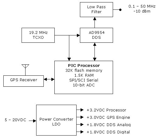
Block Diagram Design Depreciated - This design has been replaced with the next version of the HF-APRS hardware, however, this section is retained for historical reference. Starting in June of 2004, this design flew on the ANSR-19, ANSR-20, ANSR-25, ANSR-28, and ANSR-33 flights. The following is the block diagram of the HF-APRS system exciter. The exciter generates a -10dBm signal that can be amplified by band tuned amplifier or a single, broad-band class A amplifier for low power operation. A separate exciter and power amplifier stage are utilized to reduce filtering and isolation requirements as well as allow easy updates to the amplifier chain. The spectral emissions of the exciter stage are excellent. In this design, the internal sampling rate is set to 384MHz (19.2MHz TCXO reference * 20). For a 55MHz carrier, the nearest image would appear at 329MHz (384 - 55). This is easily eliminated by a simple, 7 element elliptical low-pass filter. The worst case narrow band SFDR (Spurious Free Dynamic Range) is 80dBc with a typical value of 88 - 92dBc. The means the largest in-band spur is around -95dBm. Even with 40 dB of gain, the spur is still less than -50dBm and 80dB down from the carrier. If desired, additional filtering could be added after the power amplifier. The TCXO (Temperature Compensated Crystal Oscillator) provides a very stable reference oscillator for the DDS and processor. The frequency is also measured using the GPS 1-PPS output. The transmit frequency is then corrected to provide transmit frequency accuracy of +/- 0.75 Hz over the entire operating temperature range.  HF-APRS Block Diagram. |
|
Copyright © 2001-2009, KD7LMO |
|
Web space provided by ESS, Inc. for all your consulting needs. |