|
|
Hardware
Design Depreciated - This design has been replaced
with the next version of the HF-APRS hardware, however, this section is retained for historical reference.
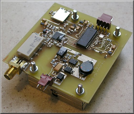
Shown below is the HF-APRS exciter board. The board is a
custom built, 2.75" x 2.75" double sided circuit board. The
board contains the processor as well as the power converter, reference
oscillator, DDS (Direct Digital Synthesizer), matching network, and output
filter.
 Programming
Port In-circuit serial programming port for PIC18F252 processor.
Software developed in
C programming language. Programming
Port In-circuit serial programming port for PIC18F252 processor.
Software developed in
C programming language.
Embedded
Processor
Microchip PIC 18F252 flash memory based embedded processor running at 19.2MHz.
Switching
Regulator High
efficiency power converter. Heat sink not required. Provides
3.2 VDC for the processor and subsystems. Typically operates from a
7.2VDC Lithium ION cell or 2 - 3.0VDC Lithium camera batteries.
19.2 MHz
TCXO A Temperature Compensated Crystal Oscillator provides a
stable 19.2 MHz reference to the DDS and processor. A single
oscillator was utilized to avoid interference between two separate clocks.
The output of the TCXO is a 1 volt peak-peak clipped sine wave, rather than
a typical rail to rail oscillator. The limited dynamic range eases
power supply bypass requirements and improves overall signal quality.
1.8VDC
Linear LDO Separate 1.8 VDC Low Drop-Out regulator provide low noise
power to the analog and digital sections of the DDS.
DDS
Analog Devices AD9954 DDS (Direct Digital Synthesizer) provides digital
generation of AM, FM, BPSK, QPSK, and SSB signals over a wide range of
frequencies. The various modulation schemes are used to generate
common signals such as Audio FSK for 1200 baud APRS, FSK for 9600 baud APRS,
and BPSK/SSB for PSK-31. With additional software, standards such as a
Pactor I/II/III and SSTV can be supported.
Output
Matching Network Broadband transformer and resistors convert the
differential current output of the DDS to a single ended 50 ohm RF signal.
Low Pass
Filter Although the DDS will generate RF signals from DC to
200MHz, a conservative 0.1 to 55 MHz design was implemented. This
supports operation in all bands from 6 to 160 meters.
All
I/O through connectors to allow for ease of installation and repairs.
Industrial temperature
range, -40° C to° C.

HF-APRS exciter board.
Board Notes - The white wire between the DDS and power converter is to
set the proper level of the digital I/O bus. In the original PCB, the
digital I/O line was wired to 1.8 VDC instead of the required 3.2 VDC.

HF-APRS exciter rear without GPS engine.
HF-APRS exciter with GPS engine installed.
Schematic / PCB Layout
For best quality, print the schematic on a single 8½ x 11" sheet of
paper in landscape mode using your favorite graphics application.
 |
 |
|
Schematic
(Graphic - GIF) |
PCB
Layout
Top Layer
(Adobe PDF) |
PCB
Layout
Bottom Layer
(Adobe PDF) |
Additional information on viewing the PCB artwork, PCB tools, and
component libraries is available in the
Technology section.
|